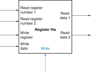
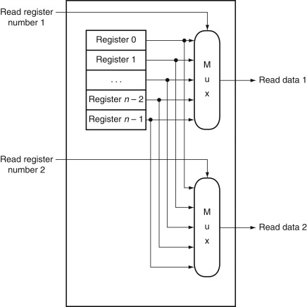
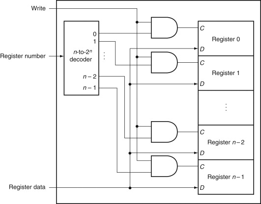
# Sequential Logic --- CS 130 // 2021-11-15 <!--=====================================================================--> ## Administrivia - Assignment 4 returned on Gradescope - <!-- .element: class="fragment"--> Assignment 5 due on Wednesday <!----------------------------------> <!-- .slide: data-background-iframe="/teaching/2021f/cs130/assignments/assignment-5/index/" data-background-interactive --> <!--=====================================================================--> # Exam 3 - Monday, November 22nd <!----------------------------------> ## Exam 3 - **Format of the exam**: + Written, in-class, 75-minute exam + Closed textbook/notes/internet + Can bring a 8.5 x 11, single-sided "cheat sheet" - <!-- .element: class="fragment"--> **Topics**: + Logic gates, truth tables, Boolean algebra, combinatorial logic, sequential logic - <!-- .element: class="fragment"--> Some of Wednesday will be dedicated to practice problems, prepping for the exam <!--=====================================================================--> # Questions ## ...about anything? <!--=====================================================================--> # Sequential Logic <!-- .slide: data-background="#004477" --> <!--=====================================================================--> ## Combinational VS Sequential - Thus, far we've built *combinational* logic circuits - <!-- .element: class="fragment"--> What is the difference between combinational and *sequential* circuits? --- - <!-- .element: class="fragment"--> **Small Group Exercise**: + Discuss definitions for "combinational circuit" and and "sequential circuit" with your neighbors <!----------------------------------> ## Responses - A **combinational circuit** is: + Relies solely on the input to resolve its output + Stateless / memoryless / doesn't depend on previous states --- - A **sequential circuit** is: + Just combinational circuits but they do save some data in memory + Thus, they **do** depend on previous inputs, etc. <!--=====================================================================--> ## Sequential Logic Components - The reading discussed four types of sequential logic components: + Clock, Latch, Flip Flop, Register,<br>and Register File --- - <!-- .element: class="fragment"--> **Is a Group Exercise** + What do each of these sequential logic components actually do? + Think, discuss, and be prepared to share <!----------------------------------> ## Responses - **Clock** + Is a signal that oscillates between 0 and 1 + The "heartbeat" of the CPU + Controls when the next instruction is executed - **Latch** + Like a "switch" that can be turned on and off + 1-bit memory unit - **Flip Flop** + Like a latch, but it changes values on the "edge" of the clock <!----------------------------------> ## Responses - **Register** + A place in memory + A grouping of flip flops that together form a single memory unit + In MIPS, have 32-bit registers - **Register File** + A grouping of registers <!--=====================================================================--> ## S-R Latch <div class="twocolumn"> <div> - A "set reset" latch is implemented with <img src='/teaching/2021f/cs130/assets/images/COD/sr-latch.png' alt="S-R latch diagram" /> - Fill in the truth table </div> <div style="font-size: 70%"> <table> <tbody> <tr><th>$S$</th><th>$R$</th><th>$Q$</th><th>$\overline{Q}$</th><th>$Q_\text{next}$</th><th>$\overline{Q}_\text{next}$</th></tr> <tr> <td>0</td> <td>0</td> <td>0</td><td>1</td><td></td><td></td></tr> <tr> <td>0</td> <td>0</td> <td>1</td><td>0</td><td></td><td></td></tr> <tr> <td>1</td> <td>0</td> <td>0</td><td>1</td><td></td><td></td></tr> <tr> <td>1</td> <td>0</td> <td>1</td><td>0</td><td></td><td></td></tr> <tr> <td>0</td> <td>1</td> <td>0</td><td>1</td><td></td><td></td></tr> <tr> <td>0</td> <td>1</td> <td>1</td><td>0</td><td></td><td></td></tr> </tbody> </table> </div> </div> <!--=====================================================================--> ## D Latch <div class="twocolumn"> <div> - A "data" latch is implemented with <img src='/teaching/2021f/cs130/assets/images/COD/d-latch.png' alt="D latch diagram" /> - Fill in the truth table </div> <div style="font-size: 90%"> <table> <tbody> <tr><th>$C$</th><th>$D$</th><th>$Q_\text{next}$</th></tr> <tr> <td>0</td> <td>0</td> <td></tr> <tr> <td>0</td> <td>1</td> <td></tr> <tr> <td>1</td> <td>0</td> <td></tr> <tr> <td>1</td> <td>1</td> <td></tr> </tbody> </table> </div> </div> <!--=====================================================================--> ## D Flip Flop - A (falling edge-triggered) **D flip flop** can be implemented with two D latches in series - The left latch is commonly called the **leader** and the right latch is called the **follower** - This configuration creates a **delay** so that the output is only changed on the **falling edge** of the clock <img src='/teaching/2021f/cs130/assets/images/COD/d-flip-flop.png' alt="D flip flop diagram" /> <!----------------------------------> ## D Flip Flop - Suppose we wanted to create a **rising** edge-triggered D flip flop. - What would need to change in the diagram below in order to achieve this behavior? <img src='/teaching/2021f/cs130/assets/images/COD/d-flip-flop.png' alt="D flip flop diagram" /> <!--=====================================================================--> ## Registers - A **register** is a multi-bit memory component - Registers are commonly implemented with an array of D flip flops <!--=====================================================================--> ## Register Files - A **register file** consists of an array of registers that can be read and written to  <!----------------------------------> ## Register Files - **Reading** is implemented with multiplexers  <!----------------------------------> ## Register Files - **Writing** is implemented with a decoder 